1 - Introduction
The first prototype is build for the MegaSTE. Why ? Because that's the machine I have.
Once this proto works I'll work on making a STF and STE version.
The goal is to first run the 68020 at the machine bus speed (8 MHz or 16MHz on a Mega STE).
To make this work some 68020 signals need to be synthesized as well as some 68000 signals.
I looked at a few existing cards like the LUCAS for Amiga and the Booster 020 from Jean Conter.
There is also a good application note from Motorola on how to interface a 68020 with a 68000
system, which is what the ST is. The Motorola application note is AN944.
So why make a new card ? ... Because I want to learn.
2 - Current prototype
The current prototype use a PGA socket for a 68020RC. It has a bunch of jumper to first make it
work at the machine bus speed so no trick on the clocks and no need to resync DTACK or any signals.
Once that work the next step is to have the 68020 run a constant speed, 32MHz in this case.
The difficulty with the Mega STE is that it boots at 8MHz and latter on switch to 16MHz. So the
cycle resync is not going to be the easiest one.
If I can't get this to work, I'll at least use the same trick as the booster v2 from exxos, switch
the cpu clock to 32MHz when not accessing the ST ; so when code is running from the cache, or when
accessing the 32 bits address space.
On the prototype I also put an expansion connector with all the signals from the 68020 so that I can
then work on putting the TOS on 2x 16 bits EPROM to get a 32 bits access to the TOS.
3 - Signals resync
- /AS :
The 68020 runs in 3 full clock cycle (6 states) as opposed to 4 (8 states) for the 68000. Motorola recommend to delay /AS by 1 bus clock cycle to align it with the standard 68000 S2 cycle. That being said, I saw that the Booster 020 doesn't do this, which mean the ST might be able to accept a 6 state cycle instead of 8. This will require testing but it can be interesting if that's the case. - /DTACK to /DSACK1 :
We also need to resync DTACK to DSACK1 if the CPU run at a different speed than the bus. As the Mega STE changes frequency this will requires some tricks. As said above, not sure yet how that's going to work. - /BG :
We need to prevent /BG to go to the ST to quickly.We will gate it on /AS to make sure we don't assert /BG to the ST if /AS is isolated from the bus (access to non ST address space or future fast TOS). - /VMA and E clock:
We need to synthesize these signals from the 68020 and the system clock. The Motorola application note has all the information we need. I also looked at the LUCAS code and the Booster020. I'll do a few test and keep the "best" one.
Future
- 4/8/16 MB of SRAM

This is the current MegaSTE prototype board as it was sent to the PCB house.
The board should be back by the end of July (2015).
I use an ATF1502 for the logic. The CPU is a MC68020RC33 PGA (fairly easy to find on eBay and cheap).
The card uses a PLCC plug (Winslow W9305)
to interface with the MegaSTE 68000 socket. This is somewhat hard to find and not cheap ( ~ $50 including shipping).
I also added an expansion port so that I can prototype the 32 bit TOS and the SRAM.

The PCB has arrived. Now time to solder.


The PCB is now assembled. I now need to finish the CPLD coding and start the testing and debugging. There are a few jumpers as you can see. These are used to route some signals either directly to/from the 68020 to/from the 68000 socket or via the ATF1502. As the goal is to first get this working at bus speed, only some signals need to be routed to the ATF1502 to generate the "missing" 68020 signals. Once that work the jumper will allow me to route more signals to/from the 68020 and 68000 bus via the ATF1502 to try to get the CPU to run at 33MHz all the time. There might be an intermediary state where I'll use the frequency switching code from the Booster V2 to switch between 33MHz and the bus frequency.
I was able to run the first test in the MegaSTE. So it doesn't work .. yet. I could see some bus cycle after fixing some of the CPLD code. I think there might be a few errors in the code for the Motorola application note AN944. I was able to fix the /AS00 timing (that the /AS that goes to the mother board) and make sure it was properly delayed to match the S2 cycle. Also the AN944 equation seem to have the output of AS00 inverted, at lest it was inverted on my logic analyzer output. So there is progress and it seems to start booting as I see TOS access (/CE of ROM is triggered and match /AS00 and /DTACK). I've noticed that /BG is doing something really weird as it follows /DTACK !!! If I disconnect the cpu /BG20 signal from the mother board the signal is a steady HI for the length of my sampling but the ST_BG (so from the mother board) still shows the weird signal following /DTACK. If I put back the 68000 on the machine and sample the same signals /BG is fine. So there is something weird going on there and I need to investigate. I might have some time to do more test next weekend.
Full 7 seconds run then crash

Zoom on crash
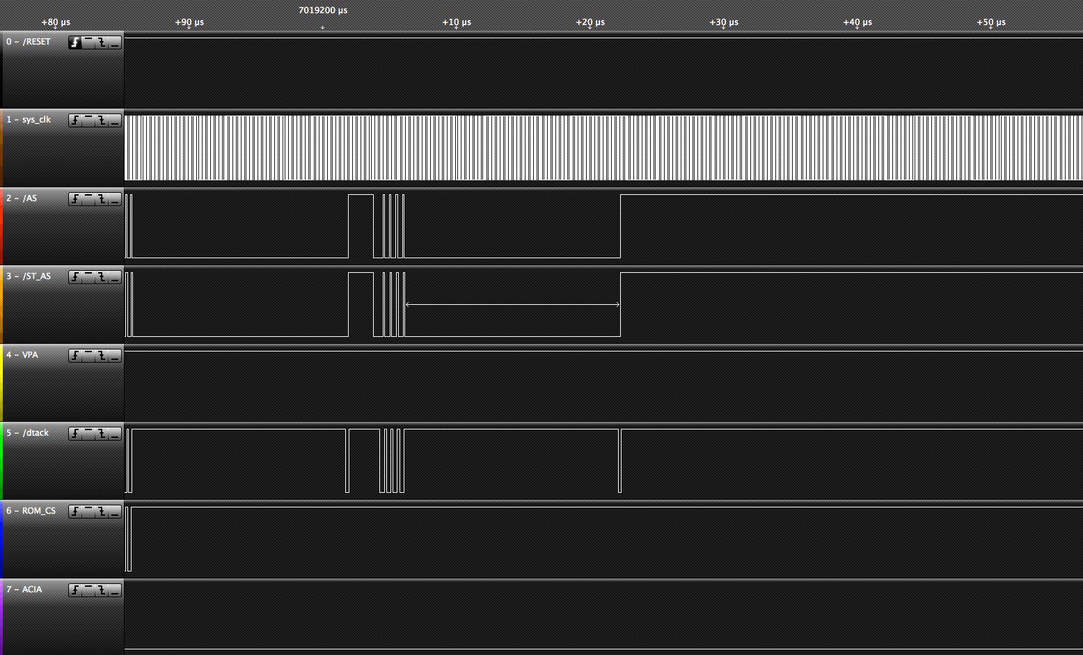
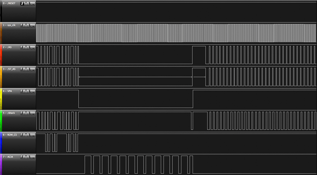
So I spent time this week reviewing the equation, make some fix and tweak. The machine obviously boot on the TOS but crashes after 7 seconds.. which is not right as the MegaSTE with the 68000 displays the Atari logo after 4s or so. So something is not responding on the bus and the CPU keeps trying .. I guess until it gets a bus error. I checked that /VPA is asserted when accessing the ACIA (see ACIA access trace). DTACK (connected to DSACK1) also respond properly. /ST_AS is delayed by 1 half clock cycle as expected to land on S2 of the 68000 bus cycle. At this point I'm a little bit in the dark as to what is going on as the card seems to work as it boots the TOS. I used my Saleae to get proper timing as I discovered that the Open Bench logic sniffer was giving me wrong timing even when sampling at 200MHz (25 times the 8MHz bus frequency).

/ST_AS, /LDS, /UDS

/VPA and /VMA no ACIA

/VPA and /VMA no ACIA

/BG issue

More progress were made this weekend.
- First now /DSACK1 arrives at the right time and the 68020 complete the cycle in 4 clock cycle. Before, even after delaying /AS20 it was getting DTACK to early and finishing the cycle in 3 clock cycle. This is due to the fact that the ST assert /DTACK a few ns after /AS is asserted.
- The ACIA access now looks good with a proper sync on E and /DSACK0 is properly asserted. I use /DSACK0 as this is what is supposed to be used for 8 bit bus access (wired to D24-D31 which is D8-D15 of the 68000 bus).
- Now of course .. it still doesn't work. I've notice that after the 2 first access to the ACIA... there are 2 more.. I didn't see 4 access on my test (will have to recheck) so something goes wrong here. Also I thing I use /CS2 on the Midi ACIA and then realize it was tie to VCC.. so that test is not valid. I'll have to recheck the ACIA access next week (if I can work on this next week).
- 2nd problem is /BG... as previously seen, when my card is on the bus, /ST_BG seem to follow /DTACK... even if I remove the jumper connecting either the CPU /BG or the ATF1504 ST_BG_OUT to the ST_BG pin ... I check with the 68000 and this doesn't happend.. so there is a problem somewhere on the card. I haven't found any shorts that would explain this. So now I need to trace all the track with a multimeter to see if I can find the issue.

weird pulse 2

Weird issues
- We made some code changes to only use DSACK1 for all transfers (MrMartian from the Atari Age forum helped me on this) including the ACIA. So far it all looks good and the cycle are termination as they should.
- Now, that being said .. it still not boot. The BG issue seemed to be solved (I cleaned the PLCC socket on the mother board as there might have been some corrosion). but now we see weird pulse in the middle of a LO or HI on some signals (seen image above). We don't yet know if it's an issue with the board (interferences), issues with the ATF1504, issues with some signal from the ST (MegaSTE in this case).
- We see these on SIZ0 and SIZ1 which come straight from the CPU. I tested with 5 different CPU... exact same result on all of them.
- So I (we) need to identify where these issue are coming from (might be false signal and just a bug in the software as I enable the analog trace on the logic analyzer and the voltage is way bellow a logic 1 for TTL, CMOS or even 3.3v CMOS/TTL. So as you see, more work to do. I might have to make a new board with some inline resistor to help with signal ringing and other issues (33 ohm inline on control signal to ATF and from ATF to ST). I might try to spend more time on this card this weekend and see if we get somewhere. If not.. time for a new board with more signal cleaning options :)
GEM Bench v4.03        Ofir Gal - 3 March 95
============================================
Mega STE  TOS 2.06
AES v3.20
GEMDOS v0.32
MiNT not present
Blitter Enabled
NVDI not present
Video Mode: 640*400*2
FPU not present
Run and Malloc from STRAM
Ref: STE + Blitter, ST High
============================================
GEM Dialog Box:             5.485    100%
VDI Text:                   5.315    103%
VDI Text Effects:          10.665    138%
VDI Small Text:             5.840    104%
VDI Graphics:              11.255    209%
GEM Window:                 1.530    103%
Integer Division:           1.560   1153%
Float Math:                10.735    124%
RAM Access:                 2.945    213%
ROM Access:                 2.535    248%
Blitting:                   1.720    106%
VDI Scroll:                 3.970    107%
Justified Text:             5.105    106%
VDI Enquire:                2.480    107%
New Dialogs:                7.010    108%
============================================
Graphics:                            117%
CPU:                                 434%
Average:                             201%
The main issue was a problem on /DSACK0. In the code we were setting the DSACK0.oe to 0 to disable it as we don't need it in the current code.
But somehow this wasn't working thus driving /DSACK0 to 0 all the time. This meant that the 68020 always saw the bus transfer as a 32 bits transfer
instead of 16 bits. Once this was found by Juliusz, the card started working and we had our first boot to desktop.
MegaSTE 68000 at 16MHz with 16K cache                   MegaSTE 68020 at 16MHz with 16K cache

GEM Bench v4.03              Ofir Gal - 3 March 95      GEM Bench v4.03              Ofir Gal - 3 March 95
============================================            ============================================
Mega STE  TOS 2.06                                      Mega STE  TOS 2.06
AES v3.20                                               AES v3.20
GEMDOS v0.32                                            GEMDOS v0.32
MiNT not present                                        MiNT not present
Blitter Enabled                                         Blitter Enabled
NVDI not present                                        NVDI not present
Video Mode: 640*400*2                                   Video Mode: 640*400*2
FPU not present                                         FPU not present
Run and Malloc from STRAM                               Run and Malloc from STRAM
Ref: MSTE + Blitter, ST High                            Ref: MSTE + Blitter, ST High
============================================            ============================================
GEM Dialog Box:             4.745     96%               GEM Dialog Box:             5.220     87%
VDI Text:                   5.040     99%               VDI Text:                   5.605     89%
VDI Text Effects:          12.250    100%               VDI Text Effects:          11.400    107%
VDI Small Text:             5.520     99%               VDI Small Text:             6.170     88%
VDI Graphics:              14.230    100%               VDI Graphics:              11.055    128%
GEM Window:                 1.340     98%               GEM Window:                 1.410     93%
Integer Division:           8.815    100%               Integer Division:           3.095    286%
Float Math:                 7.170    101%               Float Math:                 7.130    101%
RAM Access:                 3.155     99%               RAM Access:                 2.005    157%
ROM Access:                 3.145    100%               ROM Access:                 2.030    155%
Blitting:                   1.740    100%               Blitting:                   1.785     97%
VDI Scroll:                 3.925    101%               VDI Scroll:                 4.135     96%
Justified Text:             4.850    100%               Justified Text:             5.310     91%
VDI Enquire:                1.755     94%               VDI Enquire:                1.790     93%
New Dialogs:                6.065     95%               New Dialogs:                6.325     91%
============================================            ============================================
Graphics:                             98%               Graphics:                             96%
CPU:                                 100%               CPU:                                 174%
Average:                              98%               Average:                             117%
GEM Bench v4.03              Ofir Gal - 3 March 95
============================================
Mega STE  TOS 2.06
AES v3.20
GEMDOS v0.32
MiNT not present
Blitter Enabled
NVDI not present
Video Mode: 640*400*2
FPU not present
Run and Malloc from STRAM
Ref: MSTE + Blitter, ST High
============================================
GEM Dialog Box:             4.840     94%
VDI Text:                   4.510    111%
VDI Text Effects:           9.145    134%
VDI Small Text:             4.875    112%
VDI Graphics:              10.275    138%
GEM Window:                 1.380     95%
Integer Division:           1.560    567%
Float Math:                10.705     67%
RAM Access:                 2.940    107%
ROM Access:                 2.075    151%
Blitting:                   1.650    105%
VDI Scroll:                 3.575    111%
Justified Text:             4.450    109%
VDI Enquire:                2.295     72%
New Dialogs:                6.340     91%
============================================
Graphics:                            106%
CPU:                                 223%
Average:                             137%
We've made some progress on running at constant 32MHz.. but it crashes on memory test and other bus access.
So not there yet. We're also running into issues with the CPLD IDE (WinCUPL) that make coding on this very ... painful to be polite.
So we've made the decision to do a v2 board and use a Xilinx CPLD : XC95144XL (100-pin TQFP). This means a new round of board,
learning to solder these with my new reflow oven (aka learning to lay down the solder paste in the right quantity then fix bridges between pin),
learning the Xilinx tools (and VHDL)...
So we're making progress and learning from our mistakes along the way.
Rodolphe
We tried 40MHz but got a black screen. So for now we're continuing with 32MHz.
We still have a few issues to fix, mostly slow rising time on tri-state pins so we need to change some pull-up from 4.7K to 1K to see if it helps. This is needed to allow us to use the expansion bus and allow a bus master on it.
The new code is fully written in VHDL using the Xilinx tools and gives us a lot more options and is easier to modify/maintain.
We still need to do a few things:
- 32 bits TOS access at 32MHz (will probably need 1 wait state with 55ns ROM).
- Blitter TOS access when the blitter is bus master (need to multiplex 32 bits to 2x 16b its)
- Fix pull-up to allow bus master on the expansion bus
Rodolphe